Engineering
China Reached the Industry's Leading DRAM Node Without EUV. It Took Four Exposures Where Rivals Use One
CXMT announced on Sunday that its fifth-generation DRAM platform has entered mass production at an 11.95-nanometer array half-pitch, matching the geometry of the most advanced nodes now shipping. It got there with deep-ultraviolet quadruple patterning, because EUV scanners cannot be sold into China — and that substitution is the whole story.
 MAI
MAI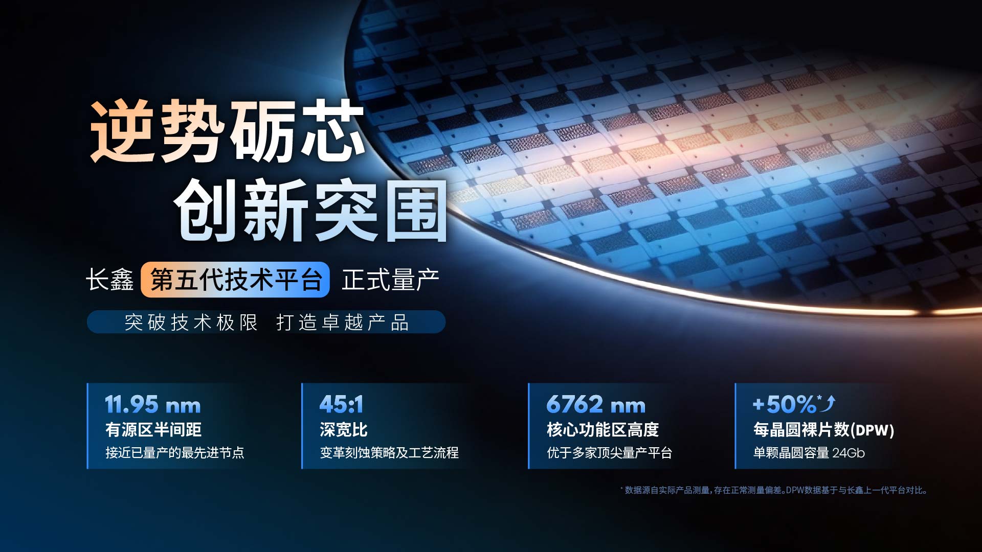
ChangXin Memory Technologies announced on Sunday, at the World Manufacturing Convention, that its fifth-generation DRAM technology platform — G5 internally — has entered mass production. The company says it has reduced the active-region half-pitch in the memory array to 11.95 nanometers, adapted a high-k metal gate process to DRAM, and shipped two LPDDR5X products built on the platform: 24Gb dies in 496-ball and 245-ball packages, aimed at mid- and high-end smartphones. Density per die is up 50 percent over the previous generation, and CXMT says G5 yields at least 50 percent more dies per wafer than G4.
Eleven point nine five nanometers puts the array geometry level with what Samsung and SK hynix are running at the 1c node, the most advanced DRAM node in volume production anywhere. That is the headline, and it is real. It is also the least interesting part of the announcement.
The number measures one structure, not a process
Analysts quoted by Korea's Seoul Economic Daily made the necessary caveat immediately: 11.95nm describes a single core dimension, and DRAM node labels — "1c", "12nm-class" — are marketing conventions that do not decompose into comparable measurements. A half-pitch figure tells you what the lithography resolved. It does not tell you the cell size, the retention characteristics, the yield, or the cost.
Two of those omissions matter more than the rest. The 50-percent dies-per-wafer improvement is a gross figure — potential dies, counted before defect screening. And CXMT did not publish a cost per bit, which is the only number that decides whether a DRAM process is competitive.
Four exposures instead of one
The reason cost is missing is visible in how the node was built. EUV scanners cannot be exported to mainland China, so CXMT resolved 11.95nm features with deep-ultraviolet quadruple patterning: a single design layer decomposed across four separate exposures, each with its own mask, each demanding overlay accuracy tighter than the feature it is placing.
| Incumbent 1c | CXMT G5 | |
|---|---|---|
| Lithography | EUV, roughly 5–6 layers | DUV, quadruple patterning |
| Array half-pitch | ~11–12nm class | 11.95nm |
| Masks per critical layer | one exposure | four exposures |
| Cost per bit | industry baseline | above baseline |
Every additional exposure adds a mask, a process step, an alignment budget and a defect opportunity. The Chinese technology press covering the launch reached the conclusion CXMT's own release avoided: generational alignment is not cost alignment. CXMT has demonstrated it can build the geometry. It has not demonstrated it can build the geometry profitably against three incumbents who reach it in one exposure.
That is a narrower achievement than "China caught up," and a more durable one than it sounds. Multi-patterning is expensive but it is not a wall. It converts a tool embargo into a margin problem, and margin problems get solved with scale and time — both of which CXMT now has more of than it did a year ago.
The shortage is paying the bill
Timing is doing a great deal of work here. DRAM is in a severe shortage: Citi projects demand growing 30 to 35 percent through 2028 against supply growth of 19 to 22 percent, as HBM and server DDR5 absorb capacity that used to serve everyone else. In a market like that, an expensive bit still sells. CXMT took 9.5 percent of global DRAM revenue in the second quarter of 2026, fourth behind Samsung, SK hynix and Micron, and it has been taking the commodity share the incumbents vacated while pivoting their fabs toward AI memory.
The market has priced this generously. CXMT listed on Shanghai's STAR Market in late July at 8.66 yuan a share, raising 57.9 billion yuan in the largest share sale in Asia this year; the stock has since risen roughly sixfold, carrying the company past Tencent by market value. Earlier this month it claimed the first LPDDR6 to reach mass production in a flagship handset, in Xiaomi's 18 Fold.
HBM is the test G5 does not answer
None of this touches the part of the memory market that is actually growing. High-bandwidth memory is where DRAM demand is concentrating, and CXMT's HBM3E is reported to be in trial production only — no volume, no confirmed customer, no official announcement from the company.
HBM is not simply advanced DRAM. It is stacked DRAM: twelve or sixteen dies bonded together with through-silicon vias, with thermal and yield-compounding problems that a good array node does not solve. Reaching 1c geometry is a prerequisite for competing there. It is not the same as competing there.
So the honest reading of Sunday's announcement is this: China's DRAM industry has closed the lithography gap on commodity memory by spending four exposures where its rivals spend one, at a moment when a shortage makes that affordable. What it has not closed is the gap in the segment that AI is paying for. The next CXMT announcement worth reading will have HBM in the headline.
Sources: 长鑫存储第五代技术平台正式量产 实现微缩工艺新突破 (CXMT) · 长鑫存储宣布第五代DRAM技术平台实现量产 (21世纪经济报道) · 长鑫存储宣布第五代DRAM技术平台G5量产,工艺达1c节点级别 (虎嗅) · China's CXMT Starts Mass Production on 5th-Generation DRAM Process (Seoul Economic Daily) · China's memory chip giant CXMT hit fresh record, up 6 times from IPO (The Standard) · 长鑫LPDDR6率先实现旗舰手机端首发量产 (CXMT)